


Physical analysis
Dual-beam Scanning Electron Microscopy
(SEM Equipped with FIB)
In-page menu
FIB-SEM (dual-beam scanning electron microscopy), in which FIB (focused ion beam observation equipment) and SEM (scanning electron microscopy) are integrated, repeats processing and observation of the object in an intermittent manner, reconstructs a steric image from hundreds of obtained images using dedicated software, and allows a three-dimensional structure analysis.
Observation in an intermittent manner enables clear observation of the structure of any invisible area of the folded portion, interface state, and other matters.
Furthermore, from the obtained three-dimensional position information, it is possible to calculate the surface area, which cannot be obtained by surface observations.
Features of dual-beam scanning electron microscopy (FIB-SEM)
Clarifies the steric structure of material with complicated three-dimensional structure (*).
| ( * ) | Complicated three-dimensional structure: Refers to such a structure as a device with a three-dimensional structure, intercrystalline interface phase, thin film/surface treatment, distribution of diplophase in ceramics/metal, and void/clearance/pore (morphology/bonding state). |
|---|
Ultra low voltage scanning electron microscopy (ULV-SEM) capable of FIB processing can handle the following:
- Low-damage processing: cryo-stage
- "In-situ section observation" from a combination of FIB and ultra-low voltage SEM
Surface sensitive observation at ultra-low accelerating voltage (min 100 V)
SEM resolution: 1 nm (15 kV)
Capable of observing various information: shape observation (out-lens secondary electron detection)- Chemical state distribution observation (in-lens secondary electron detection)
- Composition distribution observation (in-lens backscattered electron detection)
- Transmission electron image (STEM detection)
- Three-dimensional structure observation
Capable of constructing three-dimensional structures (various SEM images, EDX, EBSP)
Capable of analyzing various three-dimensional structure information (three-dimensional distribution of specific phase, morphology of specific section, blending rate, filling degree, porosity, etc.) - In-situ observation without exposure to atmosphere at low temperature
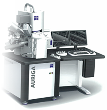
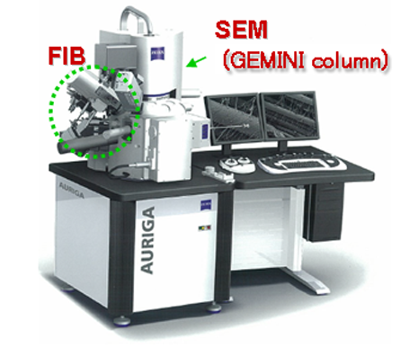
JFE-TEC uses equipment with the following main specifications
Auriga from Carl Zeiss
-
SEM function: use of GEMINI column
- Accelerating voltage: 100 V to 30 kV
- SEM detector: secondary electron, backscattered electron, STEM
- EDX detector
- EBSP detector
FIB function
- Accelerating voltage: 1 to 30 kV
-
Auriga from Carl Zeiss
Versa 3D LoVac from FEI
-
FIB function
- Beam diameter: 5 nm@30 kV
- Accelerating voltage: 0.5 to 30 kV
SEM function
- Accelerating voltage: 0.2 to 30 kV
Option: cryo-processing of the sample
- Model PP3000T from Quorum
Cryo-function and atmosphere control function
Maximum cooling temperature: -192℃ - Vacuum mode SEM
-
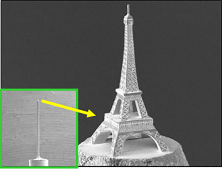
Eiffel Tower at the tip of W wire processed by FIB
Observation example
- Observation of Composite Particles/Filler by Combination of FIB and ULV-SEM
- Observation of Power Generation Layer (ZnO/Pigment Composite Layer) of Pigment-Sensitized Solar Cell (Organic Solar Cell) Using FIB-ULV-SEM