


Physical analysis
Visualization of Atoms by Aberration Corrected Scanning Transmission Electron Microscope (Cs-corrector STEM)
JFE-TEC provides services of nano-scale microstructure analyses using Cs-corrector STEM.
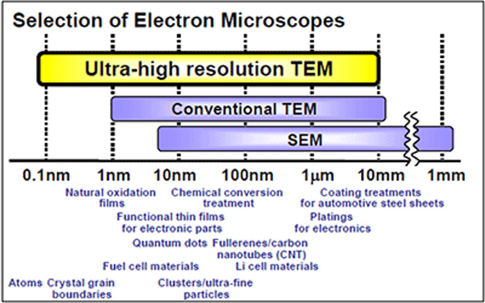
Cs-corrector STEM is a powerful tool to provide observation of ultra-micro portion such as 0.1-nm scale which is one digit smaller than the conventional TEM (Transmission Electron Microscope) in the field requiring nano-level microstructure design such as batteries and electronic parts (LSI, light emitter).
JFE-TEC provides a new perspective for client's material development and/or trouble shooting with Cs-corrector STEM which has capabilities of atomic/molecular level observations/analyses.
Features of Cs-corrector STEM
-
Equipment: ARM-200F made by JEOL
-
Capable of atomic image acquisition from 60 kV (max. 200 kV)
Resolution of STEM: 0.08 nm (conventional STEM: 0.2 nm)
STEM imaging by HAADF-ABF detector -
Capable of observation with less damaging
Low acceleration voltage observation at 60 kV
Observation using cryo-stage -
State-of-the-art analysis function
Energy resolution capability < 0.4 V with cold-cathode electron gun
High speed analysis with dual EELS and large aperture (100 mm2) -
Extensive optional functions and peripheral equipment
Non-exposure to atmosphere and 3D tomography
Cryo FIB-SEM and glove box
Ar ion milling
-
Capable of atomic image acquisition from 60 kV (max. 200 kV)
-
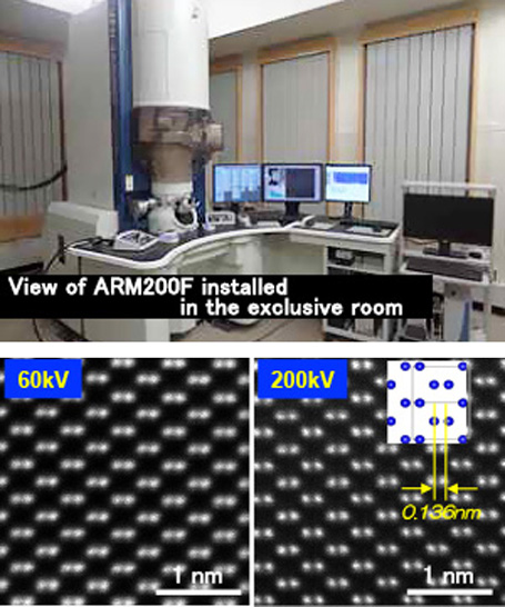
STEM images of {110} face of Si single crystal observed at 60 kV and 200 kV
(White dots: Si atoms; figure on upper right is a structure model.)
Area of application
Electronic materials:
- Lamination structure analysis of superlattice and multi-layer thin films
- Microstructure analysis of electronic parts such as LSI, LED, etc.
- Observation of magnetic heads, and quantum dots/quantum wires
Metals and ceramics materials:
- Observation of surface modification layers and oxidation layers
- Analysis of micro-precipitates and grain boundary segregations
Battery materials:
- Observation of positive/negative electrodes of Li-ion secondary batteries
- Observation of catalysts for fuel cells
Surface treatment:
- Analysis of coating films, interface structures and joining layers of surface treatment materials
Micro-particles:
- Observation of shapes and observation of micro-particles of catalysts